Creating an API for FPGA Developers
High3 Level Summary
High3 Level Summary:
The Fixed Port Flat Architecture Design Pattern is a synthesizable hardware architecture and design strategy suitable FPGA development using procedural programming techniques. The design pattern increases FPGA design productivity by introducing utilizing a form of code reuse which we call
'
architectural framework
reuse'. We motivate the need for a design pattern with a flat architecture, then describe its development using a state machine an abstract facade object. We also demonstrate the design patterns usefulness and productivity features by development of our own FPGA design entry tool,
SpeakHDL
.
Added Value
Sed ut perspiciatis unde omnis iste natus error sit voluptatem accusantium doloremque laudantium, totam rem aperiam.
Need For A Design Pattern
Need For A Design Pattern:
A
software design pattern
is defined as "a general reusable solution to a commonly occurring problem within a given context". The context in our case is FPGA development, and the problem we wish to address is FPGA design complexity. Our plan is to
port
a software design pattern over to hardware in hopes that it will help us become more productive.
In terms of software jargon, a
facade pattern
falls under the category of a
structural design pattern
. It's goal is to hide the complexities of an underlying system by providing
client classes
with a uniform interface to access
subsystem classes
that reside internal to the system. One way to achieve this goal is to introduce a so-called
facade object
.
A facade pattern is typically used when:
-
A system is very complex or difficult to understand
-
The abstractions and implementations of a subsystem are tightly coupled.
-
A simple interface is required to access a complex system

Although the facade design pattern was made for software classes and not hardware components, we see that our situation is very similar. FPGA designs are very complex and difficult to understand. We are required to
'think hardware'
all of the time, so indeed our abstractions and implementations are tightly coupled. What we need is a
meaningful
facade object that can be used as a simplified interface to underlying FPGA hardware resources. Using a facade object would also open the door to the possibility of writing an API to simplify the FPGA design process.
Facade Pattern Modification for Hardware
Facade Pattern Modification for Hardware:
Now we wish to adapt the software version of the facade design pattern for FPGA hardware design. In our modified version, we do not have '
client classes
', we have FPGA modules (
vhdl entities
). We do not have '
subsystem classes
', we have FPGA hardware components. In addition, we would like to have a little more flexibility with our modified hardware version of the design pattern vs. the original software version. So, just having a facade object at the port interface will not be enough.
The use of a facade object will give our FPGA modules decoupling from the rest of the FPGA hardware, which we like. However, we would
also like for our modules have the capability of talking directly to the outside world.
In addition, we would like to have a way to logically identify our modules in a manner that would be suitable for scripting <generic>. That means, in contrast to the software version of the design pattern where client classes just contained the single facade object, the interface to our FPGA modules needs to contain three things:
- The facade object
- I/O signaling destined directly to the FPGA pins
- A logical identifier
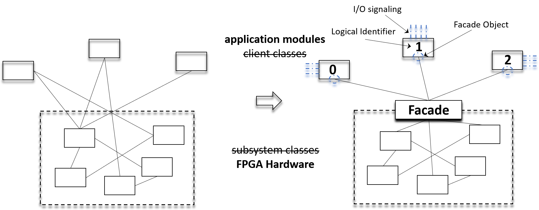
Now that we have made some high level structural modifications to the software design pattern to fit our use case, we need to discuss what our facade object will actually be. We also need to discuss what are the FPGA hardware components that the facade object will give us simplified access to.
State Machine As a Facade Object
State Machine As a Facade Object
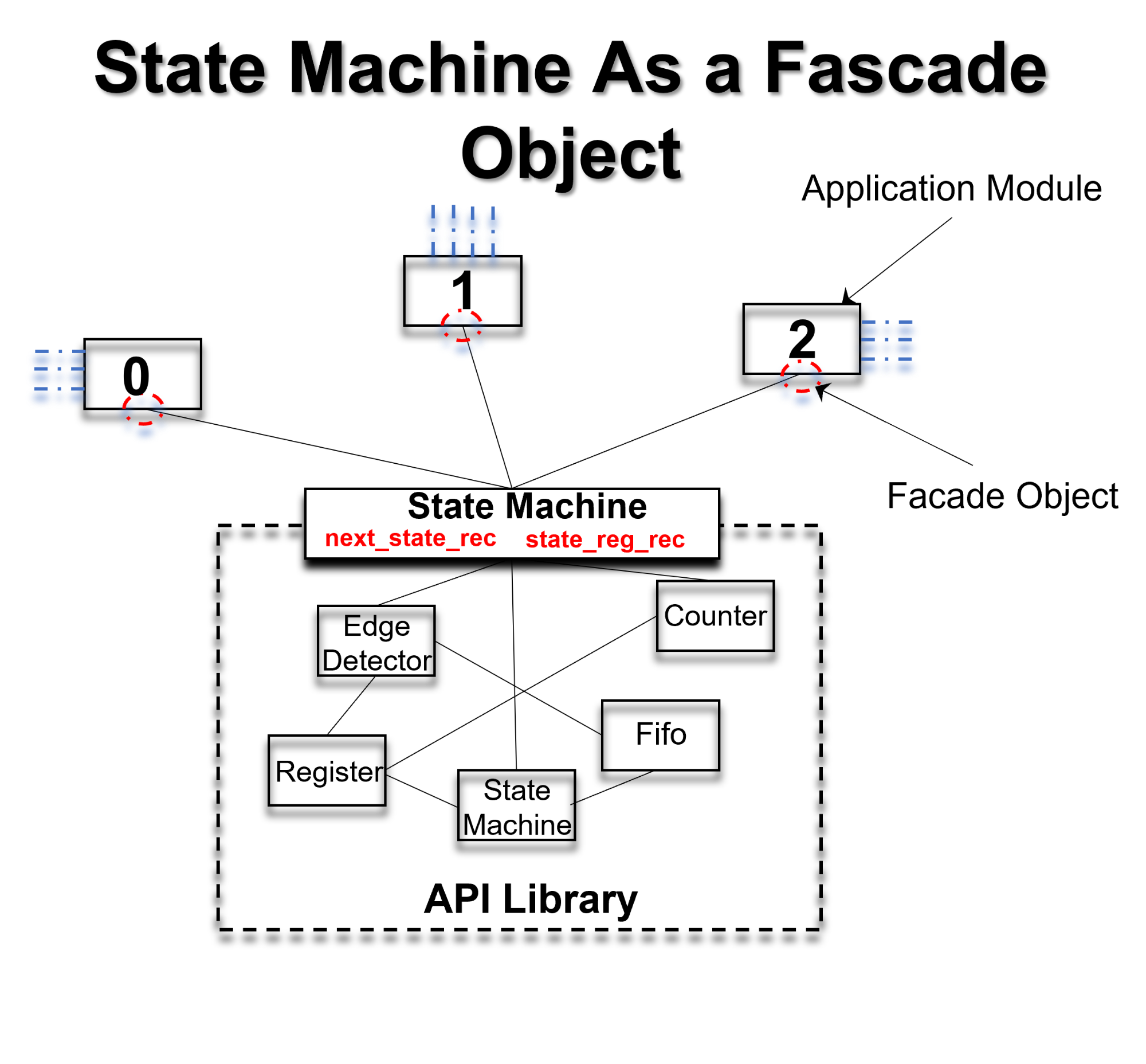
In order for a facade object to be meaningful, it must provide a "
unified interface to a set of interfaces in a subsystem
"
. In our FPGA design use case, the 'subsystems' that we wish to interface with are actually basic
hardware components
. These hardware components are the registers, counters, fifos, ect., that help us build up and interconnect the entire FPGA design. That being said, it means that our facade object would need to be an abstraction that generalizes the interfaces to these hardware components. With some clever observation, we will see that a state machine is a
great
candidate be our hardware facade object.
In order to conceptualize the usefulness of a state machine as a facade object, it helps to understand that a ny synchronous logic hardware component can be viewed as a state machine . The best way to visualize the situation is probably just to sketch out a few components. What we will notice is that each synchronous hardware component is just specific configuration of a state machine with a different 'hardware interface' as its next state logic function.
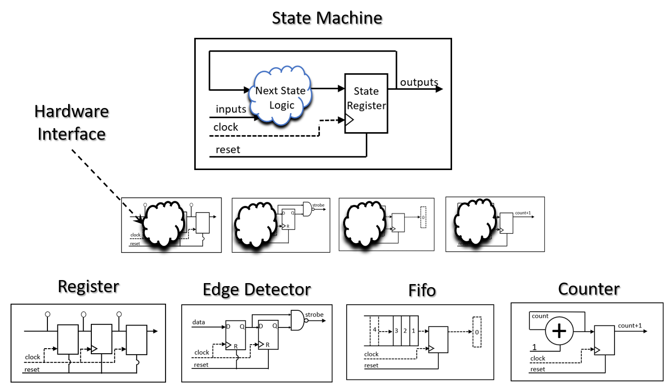
Although it may be unobvious just from a few sketches, we have actually made a huge stride towards lowering the complexity of our FPGA designs. By using a state machine as a facade object, we can now mask the complexity of how a particular hardware component is configured and expose a consistent interface to the developer that is configurable by simple API calls.
There is still a little that we need to perform, but, here is an example of something we will be able to do. Consider the following two code snippets of a counter:
           if (clk'event and clk = '1') then


           if (reset = '1') then


           count_reg <= (others => '0');


           if (count_reg < 25 and count_en = '1') then


           count_reg <= (others => '0');


           elsif (count_en = '1') then


           count_reg <= count_reg + 1;


           end if;


           end if
CONFIGURE_COUNTER( 0, 25, -1, next_state_rec, state_reg_rec, count_en );
Both VHDL code snippets do exactly the same thing. They both infer a counter. When enabled, both counters increment on every clock cycle and rollover after the count reaches twenty-four.
Which code would you rather use?
Now that we have covered some preliminaries and have seen some example API level code that we would like to get to, we now would like to formally introduce the Fixed Port Flat Architecture Design Pattern. We will talk about some ways the design pattern increases productivity and the strategy we take when creating an API for it. We start that discussion with how the design pattern gets its name.
As an example, let's say we have a FPGA module and would like to configure a counter. On the application side, the developer interacts with the hardware strictly in terms of an API call, '
CONFIGURE_COUNTER'
, that configures the
next state logic
and returns the
state registered logic.
The developer need not be concerned about what happens "under the hood". All of the details of how the counter is actually implemented are abstracted away.
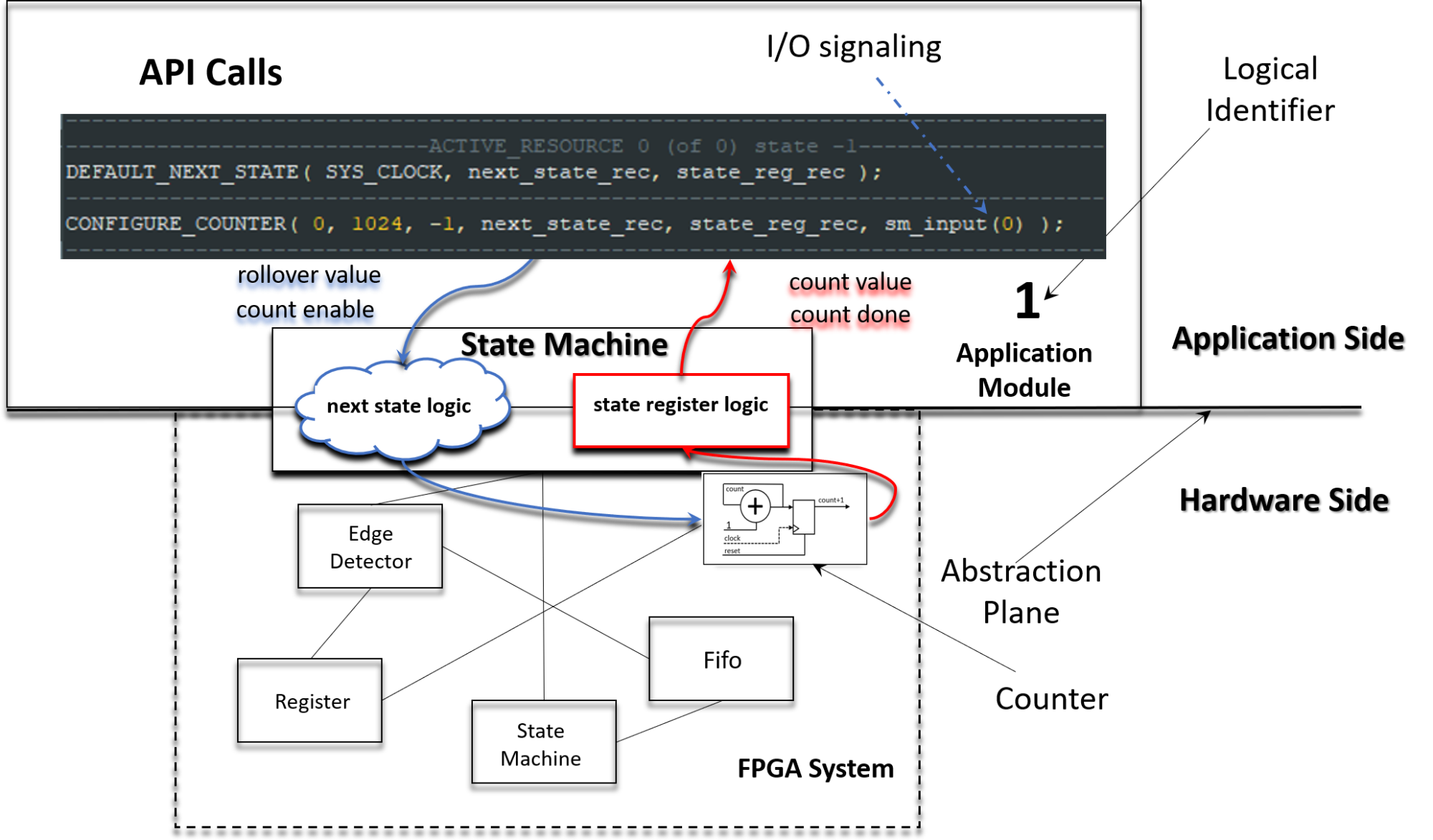
On the FPGA hardware side, however, we are left to deal with the complexity of how the hardware is actually configured. Each of the different components made available to the developer by API call will need to be implemented in VHDL code and placed inside a library. In addition, we are still on the hook to create an architecture that will support receiving these API calls.
State Machine As a Facade Object A Closer Look
State Machine As a Facade Object: A Closer Look
Before moving on to look at how we actually plan to make our abstraction work in hardware, we probably should 'zoom in' a little further and take another look at our state machine facade object. There are a couple things to point out that effect our resultant code VHDL code.
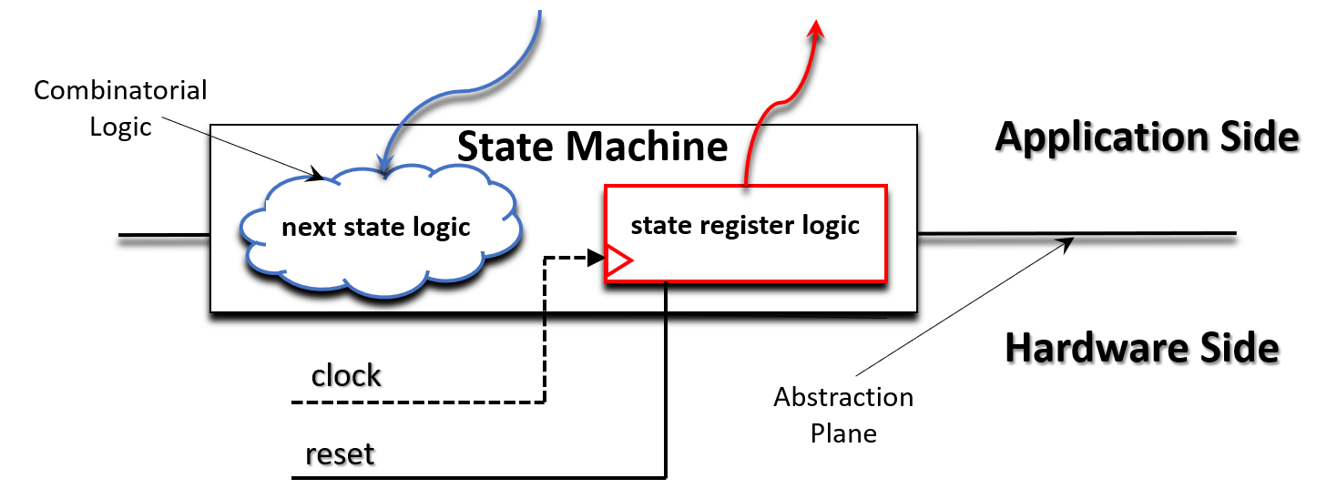
The first thing to note is that both the clock and reset signals drive the state register and are on the FPGA system side of the 'abstraction plane'. This is actually a pretty big deal that brings us productivity. It means that we have found a way to abstract the clock and reset signal away from the application developer . The other thing to note when using API calls, is the application module is only responsible for driving combinatorial logic.

An Architecture to Support Procedural Programming
- Warning
-
Lorem ipsum dolor sit amet, consectetur adipiscing elit. Duis id ligula diam.
- Item 1
- Item 2
- Item 3
- Item 4
- Note
-
Lorem ipsum dolor sit amet, consectetur adipiscing elit. Duis id ligula diam.
- Item 1
- Item 2
- Item 3
- Item 4
Need for a Framework Module
Need for a Framework Module
So far in our quest to create a low-level API to help FPGA developers to configure hardware, we focused on replacing the facade design pattern software abstractions with suitable hardware abstractions. By using a state machine as a facade object, we have created a consistent interface to where the application module can configure different hardware components using convenient API procedure calls. Now we are at the place where we are forced to go 'under the hood' and resolve all the details about how to actually implement a hardware procedure call.
Because our FPGA hardware does not have an Operating System running software to receive API calls,
we need to create our own centralized hardware framework
to act in its place. The job of the framework module is to:
- Act as a call center to receive API calls from all application modules
- Infer and configure infrastructure related synchronous hardware components that are requested by application module procedure calls
- Perform logical interconnection between application modules
- Handle the clock and reset for all infrastructure related hardware components
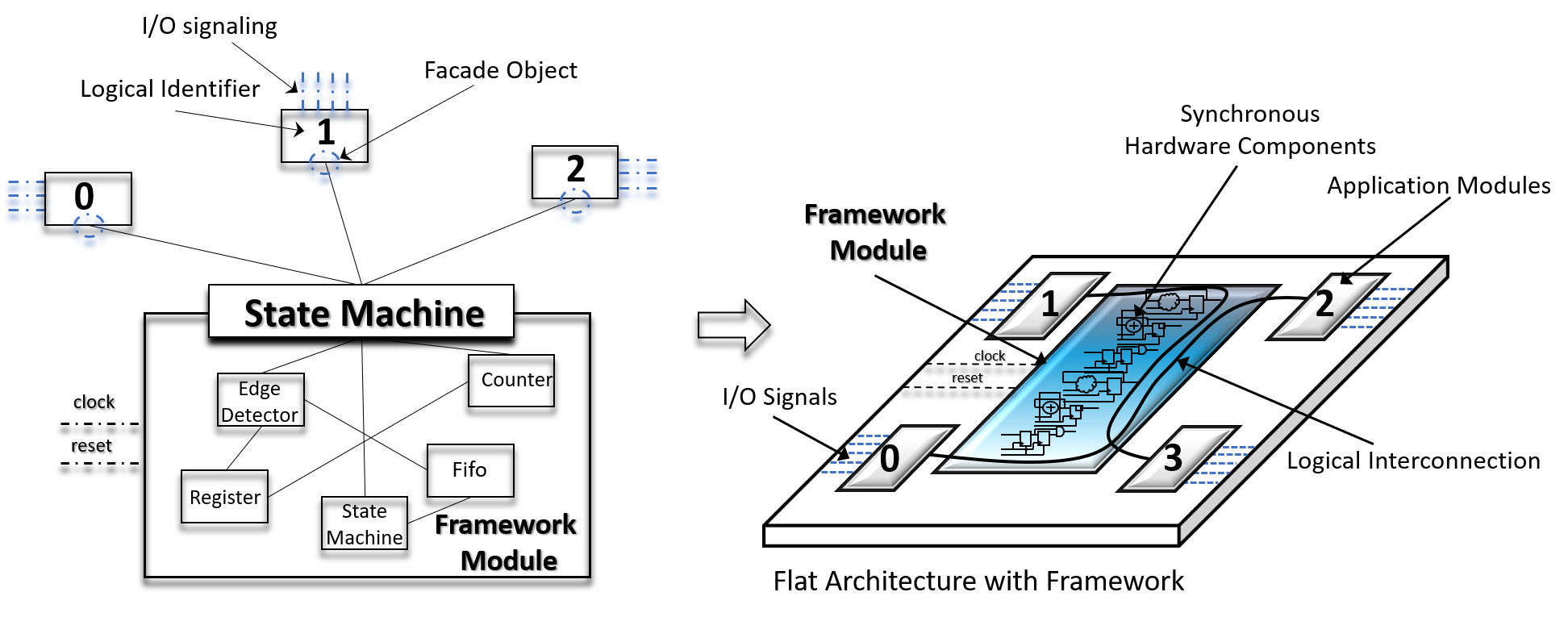
Before we continue on, there are a few things that are immediately noteworthy our framework module:
- The framework module is shared between all application modules
- The framework always operates synchronously
- The framework 'owns' the hardware that get inferred by application modules procedure calls, the application modules are just allowed to use it
Because the framework module is shared between all application modules, no one module instantiates it. It exists at the top level of the design and 'fans out' to all the application modules. Because the framework operates synchronously, it handles the clock and reset for all infrastructure related hardware components that get inferred by procedure calls. This means that if an application module only utilizes procedure calls, there is no real need to for that application module to ever interact with the clock signal or the reset signal.
Framework Module Internal Data Structures
Framework Module Internal Data Structures
Now that we have motivated the need to have framework module, and understand its purpose, we are at a place where we should discuss how data structures are organized. Inside the framework, we chose to have the state register data structures that relate to hardware components packaged into what we call an ' array of resources' . Each individual resource element is a VHDL record which may in turn contain an array of hardware components.
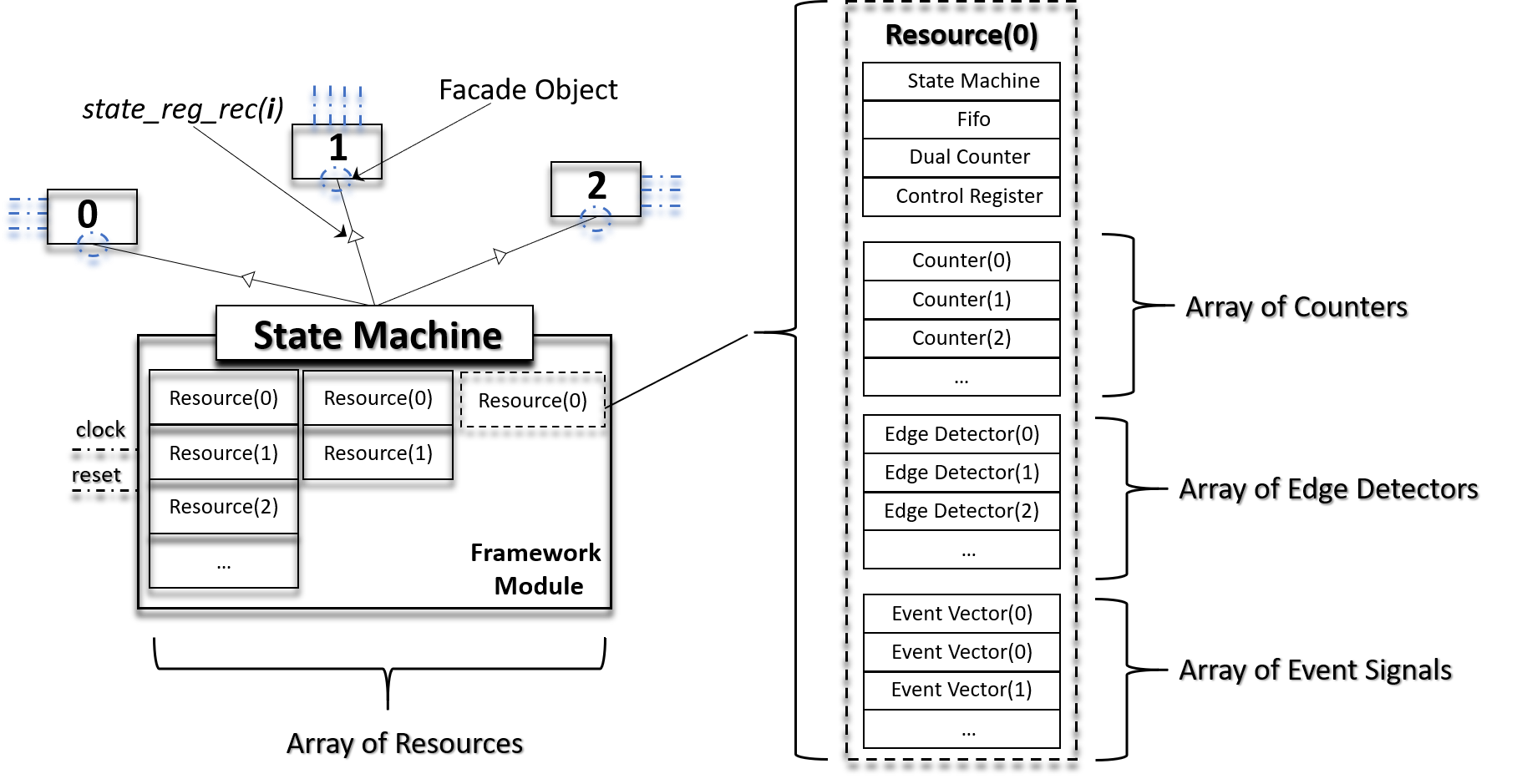
Each resource element ( for now ) contains:
- A single state machine
- A single fifo (receive buffer)**
- A single dual counter (used for timing)
- A single control register**
- An array of counters
- An array of edge detectors
- An array of event signals (used for broadcast)**
- ** Uses the framework crossbar for module interconnection
The idea is to create data structures flexible enough to accommodate a variable number of different hardware components with the possibility of adding more components in the future. This means that
the state register signal that is routed from the framework module to each application module must be a large data structure
. The design patterns usage of large data structures at the port of application modules effect the resultant VHDL code in both a negative and a positive way:
- Negative : The signal names for the state register can become rather long at times.
- Positive : There is no need for the application module to declare a signal relating to a framework component.
The fact that the signal names for the state register can become rather long is somewhat of a nuisance that we can combat by using VHDL aliases. The second artifact is actually a positive one and brings productivity. Because the state register is a large data structure that appears at the port, the FPGA developer has essentially has access to a large number of 'pre-declared' signals. This results in needing to write less signal declarations and ultimately less lines of VHDL code.
A Flat Architecture for Infrastructure Reuse
A 'Flat' Architecture for Infrastructure Reuse:
By creating a centralized framework module that was to be shared between all application modules, we introduced a newer form of code which did not exist before. We call this newer form of code reuse an
'infrastructure reuse model
' and is based on a flat design architecture. This is in contrast to the traditional hierarchical approach to achieving code reuse through component instantiations.
When we say that the architecture is 'flat', we do not mean that the architecture does not support component instantiation. We mean that geometrically, if the traditionally hierarchical component code reuse model is built up vertically, then our infrastructure code re-use model would be geometrically flat. With a flat design architecture, application modules interact with each other as loosely coupled peers instead of a traditional hierarchical parent-child like relationship.
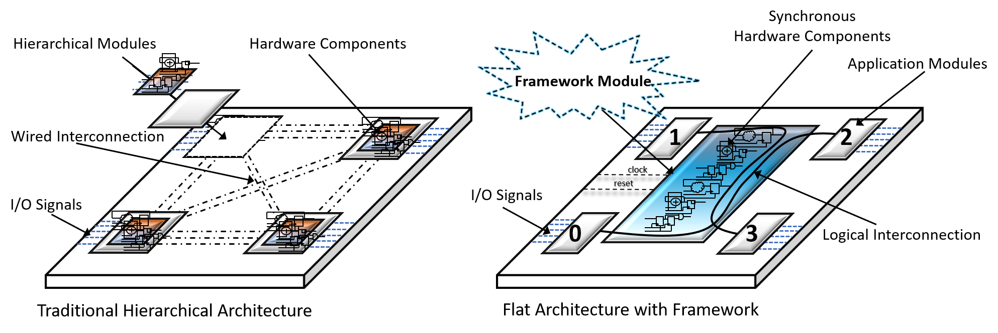
The infrastructure reuse model to achieving code reuse is through centralization of hardware resources. The framework module is deemed the orchestrator and maintainer of the centralized resources and application modules behave as clients to the framework module. Infrastructure related hardware components are made available to the application modules upon request (API call). In addition, the framework module also provides the 'wired plumbing' necessary for connection of the application modules. All module to module communication is done through framework module, however, it must be requested by an API call.
The Fixed Port
The 'Fixed Port'
Now that we have an architecture with a framework module that supports receiving API procedure calls, we wish standardize its usage. The plan to ease the burden of FPGA system design by making addition and removal of application modules as seamless as possible. In addition, would like for FPGA developers that utilize the design pattern to structure the VHDL code in a uniform way. This is done by presenting a fixed port interface that all application modules are required to conform .

Constraining the port interface of each application module to be fixed and have identical signaling to every other module has several important consequences. Notably the constraint:
- E ases the integration of individual modules at the system level
- E nforces the use of the API for module-to-module interconnect wiring
- E ncourages modules to use of API calls to infer infrastructure related hardware instead of manually coding common components
- E nhances readability of the VHDL code by promoting the use of procedure calls over the more verbose VHDL process statements
It should be noted that although the clock and reset signal enter the port of the application modules, they not utilized by the developer when using API calls. When using API calls, the framework handles the clock and reset signals for us at the top-level. The clock and reset signals are needed when the developer writes custom RTL logic or configures a custom IP core.
In addition, one of the main features of the design pattern is that it keeps application modules loosely coupled from the framework hardware, and loosely coupled from one another. This loose coupling property would being to break down if an FPGA developer were to try instantiate an application module or create custom wiring between two application modules. Fixing the port interface gives us at least some insurance that these things will not happen.

Above all, fixing the port interface allows for scripting of the top-level design entity and automated calculation of the number of resources needed by each application module. The use of scripting allows for productivity enhancing FPGA development tools to be developed using the design pattern.